Submitted by Vanessa Bismuth on Tue, 10/08/2021 - 15:56
The Cavendish’s Astrophysics Group has been awarded a £900k EPSRC grant to develop a new precision manufacturing technology based on technology developed by David Buscher, Chris Haniff and John Young to equalise the optical paths in arrays of telescopes. This will address an immediate need in astronomy for metre-scale diffraction gratings.
Over the past 25 years, precision manufacturing has become a core technology enabling the development of thousands of products. Smartphones, digital imagers, and even medical implants depend upon precision manufacturing with tolerances at the micron or sub-micron level. While tolerances at the nanometre level are possible using techniques such as electron-beam lithography, these tolerances can usually only be maintained over distances measured in millimetres. In this initiative, the group will develop the technology to push manufacturing at nanometre precision to allow it to maintain this precision over metre scales.
The first target for this new precision manufacturing technique is the manufacture of diffraction gratings for spectroscopy on Extremely Large Telescopes (ELTs) such as the European ELT (E-ELT).
Spectrographs are the workhorse of astronomy and depend upon the use of diffraction gratings to split starlight into tens or hundreds of thousands of spectral channels. These gratings consist of a large set of parallel finely spaced grooves manufactured to precisions measured in nanometres. For the upcoming generation of astronomical telescopes with primary mirror diameters of tens of metres, the gratings needed are typically metres in size.
To solve the manufacturing challenge of nanometre precision over metre scales requires a combination of two new technologies. The first is that of manufacturing nanostructures in silicon using wet etching. This has been used by groups such as Dr Uwe Zeitner's group at the Fraunhofer Institute in Jena to make centimetre-sized silicon gratings with exquisite accuracy.
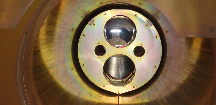
The second technology is based on the delay lines developed by the Astrophysics group for use in optical interferometers such as the Magdalena Ridge Observatory Interferometer (MROI). Optical interferometers are arrays of telescopes used to observe astronomical targets at scales much finer than possible using conventional telescopes such as the Hubble Space Telescope. The delay lines are used to equalise the optical paths between telescopes in the array and involve moving mirrors precisely over distances of hundreds of metres.
The technology used in these delay lines will be used to build a precision "lithography engine", capable of patterning silicon substrates over metre scales with nanometre precision. The lithography engine will "write" patterns on to photoresist-coated silicon wafers using a "floating head" whose position is precisely controlled with the aid of laser metrology. The patterned silicon will then be processed by Zeitner's group to yield large, accurate gratings.
The lithography engine developed through this programme can serve as the basis of a more widespread revolution in precision manufacturing. Unlike other grating-patterning technologies which project stripe-shaped interference patterns onto a substrate, the lithography engine architecture can be straightforwardly extended to allow arbitrary two-dimensional patterning over metre scales while maintaining nanometre-level accuracy. Exploring the manufacturing applications of such an extended capability is the longer-term goal of this programme.
This story is adapted from an article originally published on David Buscher’s website.
Image:
The MROI delay line trolley inside its vacuum pipe - view looking through the top port-hole at the retroreflecting mirror. The trolley can travel over 100 metres while maintaining better than 5 nanometre precision in the position of the mirror. Credit: Bodie Seneta.
