 We have developed a novel scanning probe system attached to the mixing chamber of a dilution refrigerator scanning probe. Voltages applied to the scanning probe allow us to study the details of conduction in mesoscopic device structures as well as fabricating and modifying devices by depositing charge on the wafer surface. We have used this technique for the following experimental investigations:
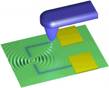
- Imaging diffraction-limited electronic collimation from a non-equilibrium one-dimensional ballistic constriction.
- Imaging cyclotron orbits and scattering sites in a high-mobility two-dimensional electron gas.
- Imaging random telegraph signal sites near a quasi 1D electron system.
- Quantum-dot electron occupancy controlled by a charged scanning probe.
- Imaging electrostatic microconstrictions in long 1d wires.
- Erasable electrostatic lithography for quantum components.
- Imaging fractal conductance fluctuations and scarred wave functions in a quantum billiard.
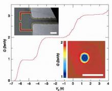
- Conductance quantisation at a half-integer plateau in a symmetric GaAs quantum wire.