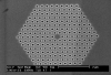
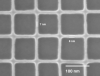
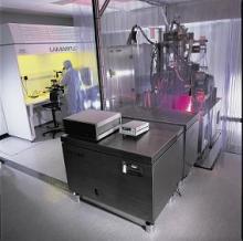
 We use a Leica VB6 UHR electron beam lithography machine for nanoscale patterning of semiconductor structures. This state-of-the-art system, which was installed at the Cavendish Laboratory in 2002, uses an electron beam of diameter 4nm and energy up to 100kV. It is capable of patterning substrates of up to 200mm diameter with a resolution as high as 10nm. This instrument is used to produce samples for a wide variety of academic and industrial users.
Examples of structures fabricated are shown