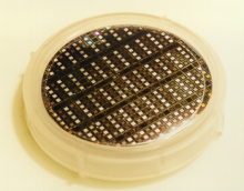
 This facility provides an extensive range of equipment for the processing of III-V semiconductor material into devices for both electrical and optical measurements. This equipment includes:
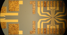
- Optical lithography for pattern formation in device structures to a resolution of around 1 micron.
- Thermal evaporation for a wide range of materials for n-type and p-type ohmic contacts as well as metal gates.
- Electron beam evaporators of both metals and insulators.
- Wet etching using a range of different chemicals.
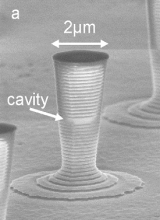
- Reactive ion etching.
- Plasma enhanced chemical vapour deposition (PECVD) of silicon nitride and silicon oxides.
- Wire bonding and electrical testing of devices.
- Atomic force microscope and Dektak for process characterization.
- The facility has around 40 regular users including users from other institutions.