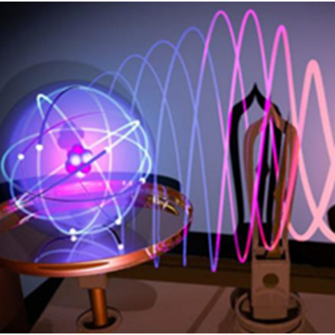
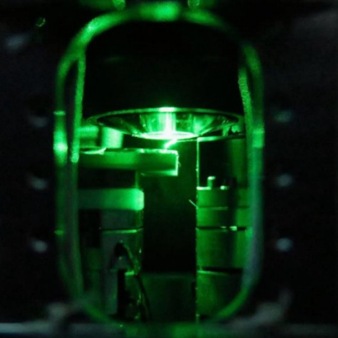
The Advanced Quantum Physics and Devices theme focuses on the design, development and testing of devices/systems that rely on the creation, control and manipulation of quantum states to deliver non-classical system performance.
The nature of these devices is exceptionally wide, ranging from optical systems whose quantum unit is the photon, to low-dimensional semiconductor-based structures to spin-based devices, but also hybrid integrative technologies such as combined photonic, magnetic and electronic integrated circuits to realise higher-level functionality.
Examples of devices include light sources, low-loss (spin-enhanced) electronics, sensors, detectors, surface probes, energy resonances for thermoelectrics.
Jump to:
Researchers associated with this theme
News and articles related to this theme
Research areas
Spin and superconductor devices
We study quantum effects in magnetically ordered materials and at interfaces between magnetic and superconducting materials using different techniques with a bandwidth that ranges from DC up to terahertz frequencies. Research Papers: Room-temperature spin–orbit torque in NiMnSb | Nature Physics | Boosting spintronics with superconductivity: APL Materials: Vol 9, No 5 | Magnonic charge pumping via spin–orbit coupling | Nature Nanotechnology | Enhanced spin pumping into superconductors provides evidence for superconducting pure spin currents
|
Nanophotonics
Confining light on the nano-scale massively increases light-matter interactions. This can be achieved with nanophotonic structures, creating regimes in which novel quantum processes for electrons and spins can be observed and exploited for enhanced device functionality. Research Papers: Single-molecule optomechanics in picocavities | Detecting mid-infrared light by molecular frequency upconversion in dual-wavelength nanoantennas | Resolving Sub-Å Ambient Motion through Reconstructions from Vibrational Spectra
|
Quantum sensors
Mass sensors and accelerometers with unrivalled sensitivity can be developed by exploiting quantum effects. For example, mesoscopic mechanical resonators can be formed from 2D materials, which offer the possibility to control motion at its quantum limit of single phonons. Diamond colour centres also offer a platform for quantum-enhanced sensors to reveal new physics in nanoscale length scales such as nanoMRI inside live cells for applications in the life sciences. Research Papers: Phys. Rev. Applied 13, 044004 (2020) - Nanoscale NMR Spectroscopy Using Nanodiamond Quantum Sensors
|
Quantum Instrumentation for Surface & 2D nanoscience
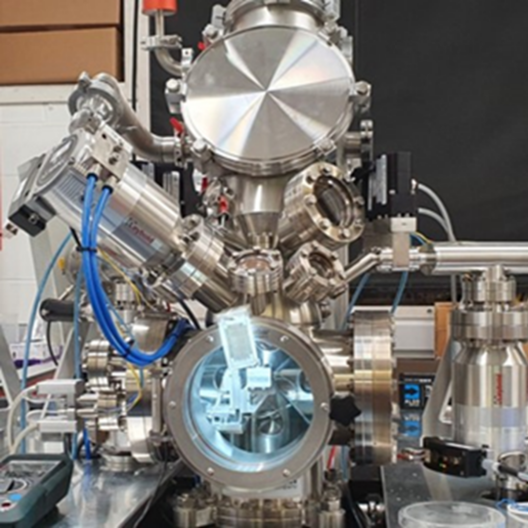
Using neutral helium matter waves enables the structure and dynamics of advanced surfaces and 2D materials to be characterised, in delicate and otherwise physically inaccessible regimes. Our globally unique instrumentation enables the discovery of novel quantum phenomena in a technologically relevant context. Research Papers: Motion of water monomers reveals a kinetic barrier to ice nucleation on graphene | Nature Communications | Phys. Rev. A 103, 053315 (2021) - True-to-size surface mapping with neutral helium atoms | Phys. Rev. Lett. 126, 155901 (2021) - Ultrafast Diffusion at the Onset of Growth
|
2D materials for quantum devices
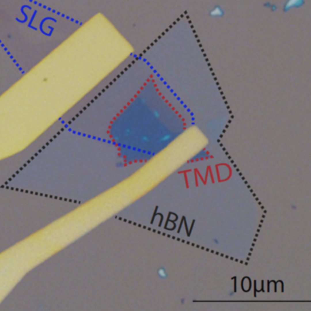
Materials which form a crystal lattice in two-dimensionals, offer a platform for storing quantum memory. Spin can be readout optically in systems including single defects in hexagonal boron nitride and bound excitonic states in transition metal dichalcogenides. This "spin-photon" interface could then be used as a basic building block for establishing a quantum internet. Research Papers: Large-scale quantum-emitter arrays in atomically thin semiconductors | Nature Communications | Room-temperature optically detected magnetic resonance of single defects in hexagonal boron nitride
|
Terahertz device physics
The three-dimensional photoelectric effect allows conversion of light to electricity in the visible or ultraviolet range, but is inefficient at much lower frequencies in the far infrared. By realising a related principle in a nanometer-thin, two-dimensional conductive layer with inhomogeneous electron density, a strong photocurrent can be observed in response to terahertz radiation by an “in-plane photoelectric effect,” yielding a highly efficient mechanism of terahertz detection. Research Papers: An in-plane photoelectric effect in two-dimensional electron systems for terahertz detection
|
Quantum effects in molecules and semiconductors
Conjugated molecular semiconductors, which are emerging as an important class of optoelectronic materials, constitute well-defined quantum mechanical systems. Their properties can be designed with a high level of versatility and synthetic control at the atomic level. We are exploring how to probe these quantum mechanical properties using a range of spectroscopic, electric and electro-optical techniques and how to control the quantum states when the molecules are embedded into a host molecular environment in the solid state. In the long term our research could lead to novel molecular quantum devices and new approaches to quantum information processing and quantum sensing.
|
Researchers and Research Groups associated with this theme


