Submitted by Administrator on Tue, 30/07/2013 - 14:50
 A Cambridge-based collaborative research project led by Dr Stefan Hofmann of the Engineering Department has been awarded £2.3M by the EPSRC (project total £2.83M) to address the manufacturability of graphene and related novel layered 2D materials and to create a basis for a lucrative high-tech graphene industry and product value chain. Dr Ulrich Keyser of the Cavendish Laboratory is taking part in this programme leading the work on graphene based single-molecule biosensors and integration of graphene into micro- and nanofluidic channels.
The Chancellor of the Exchequer, George Osborne, outlined plans to boost development of the "super-material" graphene and announced the backing for research projects recently on BBC (see eg coverage under www.bbc.co.uk/news/science-environment-20846282).
Graphene is a single layer of graphite just one atom thick - the very same material making up a pencil's "lead", but with record-breaking mechanical strength and electronic properties. Graphene is tricky to work with - sheets just an atom thick are difficult to controllably grow, to manipulate, to reliably connect to other materials. These are the key engineering challenges ahead and overcoming these bottlenecks lies at the heart of the project.
Most high quality graphene to date is in fact isolated via scotch tape from graphite flakes, as devised by Nobel prize winners A. Geim and K. Novoselov from Manchester. Such mechanical exfoliation is however entirely unsuitable for industrial production. Hence the research team at Cambridge focuses on a growth method called chemical vapour deposition (CVD) to devise a real pathway to graphene manufacture and address the key questions of industrial materials development. CVD was the growth method that opened up other materials such as diamond, carbon nanotubes and gallium nitride to industrial scale production.
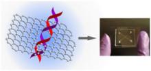
The engineering-led research project brings together a unique consortium of world leading academics, namely the groups of Dr S Hofmann, Prof J Robertson, Prof A Nathan, Dr T Wilkinson (all CUED) and Dr U F Keyser (Cavendish), as well as market-leading industrial partners that constitute the full supply chain of beneficiaries, from equipment manufacturer (Aixtron UK) to electronics and photonics companies, namely Philips, Intel, Thales and Selex Galileo. The consortium will develop novel integration routes for graphene and other layered 2D materials for a diverse set of near-term as well as future applications, ranging from advanced transparent conductors for organic light emitting diodes and liquid crystal devices, to interconnects for next generation integrated microelectronics, spintronics and lab-on-a-chip devices tailored to rapid single-molecule biosensing. This will allow new environmentally friendly solutions for general lighting, new form factors in life style electronics, improved military imaging and fire safety, and mass sensing applications in healthcare, security and environmental protection. The process technology will open new horizons for nanomaterials, built layer by layer, and thereby offers an amazing range of future devices and applications.